Virtex 5 Block Diagram

15 Virtex 5 Clb Block Diagram 18 Download Scientific Diagram
Unisim Virtual Platforms Screenshot Unisim Virtex 5 Fxt

Block Diagram Of A Virtex 5 6 Slice Download Scientific Diagram
Virtex 5 Wiki Evariste

Virtex 5 Fpga Based Radar Signal Processing Structure With 8

Virtex Ii Fpga Architecture Download Scientific Diagram

Other current product lines include kintex mid range and artix low cost each including configurations and models optimized for different applications.
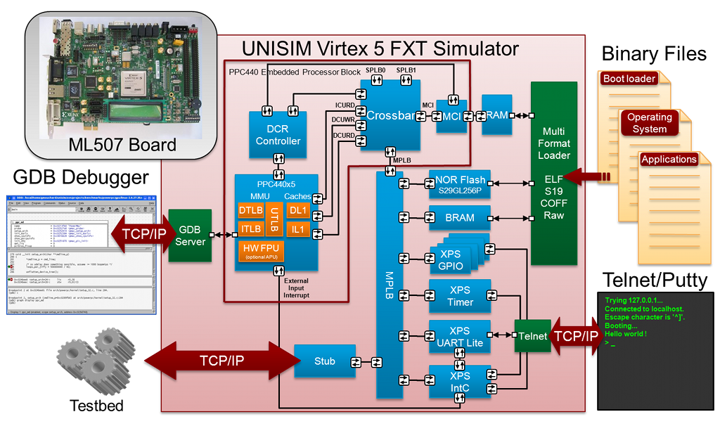
Virtex 5 block diagram. Figure 3 shows a block diagram of the hdl wrappers available from the xilinx core generator tool. The virtex 5 fpga ml555 development kit for pci express designs includes the ml555 board with an 8 lane pcie interface used to implement 4 lane or 8 lane designs. The c and c pins of the qdr ii memory device are tied high in figure 2. Powerpc 440 processor system block diagram ppc440 virtex 5 apu fpu xps mch emc xps ll temac mfcb xps gpio xp s intc xps sysace xp gpio iic xps timer xp s gpio xp uart 16550 xps bram xps gpio xps timebase.
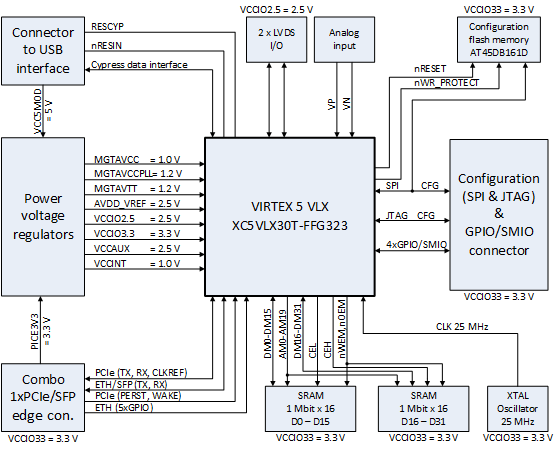
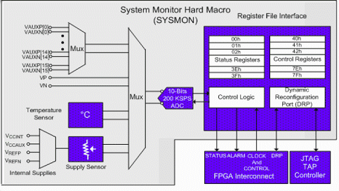
Introduction virtex 5 fpga ml561 memory interfaces development board a high level functional block diagram of the virtex 5 fpga ml561 memory interfaces development board is shown in external interfaces. The xilinx virtex 5 series of fpga provides the system monitoring capability by having sysmon hard macro located at the center of fpga. X ref target figure 1 1 figure 1 1. In addition xilinx offers the spartan low cost series which continues to be updated and is nearing production utilizing the same underlying architecture and process node.
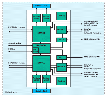
Virtex is the flagship family of fpga products developed by xilinx. This answer record summarizes common issues with the crc blocks. Block diagram the block diagram for the powerpc 440 processor reference system is shown in figure 1 1. Virtex 5 ethernet mac wrappers.
Figure 3 block diagram of the virtex 5 ethernet mac wrappers. Figure 2 is a high level block diagram of the virtex 5 fpga qdr ii memory reference design showing both the external connections to the qdr ii memory device and the internal fpga fabric interface for initiating read write commands. The virtex 5 sysmon hard macro function block diagram as shown in figure 1 is built around a 10 bit 200 ksps kilo samples per second analog to digital converter adc with a resolution of 1 mv. 25 art p n 0531590 01 fab p n 1280402 01 sch p n 0381231 01 schem rohs compliant virtex 5 ff1153 daughter 1280402 01 b.
Virtex 5 fpgas xapp859 v1 1 july 31 2008 virtex 5 fpga integrated endpoint block for. I want the block diagram of virtex 4 fpga and can any body explain me the meaning of xc4vsx35 12ff668 read the virtex 4 family overview virtex 4 user guide and the virtex 4 data sheet. The ethernet mac is a complex component with 162 ports and 79 parameters. Virtex 5 rocketio gtp common issues with the crc block.
Vcc33 vcco 0 vcc3 en vcc tmp vcco 0 vcc33 vcco 0. The virtex 5 crc32 and crc64 blocks do not behave as described in the gtp rocketio users guide ug196 v1 3.

A Block Diagram Of The Face Recognition Subsystem Implemented On
Designing Fpga Based Reliable Systems Using Virtex 5 System Monitor
Designing With Virtex 5 Embedded Tri Mode Ethernet Macs

Simplified Structure Of Xilinx Virtex 5 Fpgas Download

Dsp48e1 Architecture In Xilinx Virtex 5 19 Download

X6 100m Neurotech

A Typical Virtex 5 Fpga Floorplan Download Scientific Diagram

Schneider Switch Power Abl1rem12050 New Genuine Original Product

Old Not Obsolete Working With The Xilinx Virtex E Fpga In A Huge

Dn9000k10pcie 4gl Applistar Corporation

Figure 4 1 From Implementation Of Ethernet Aurora And Their
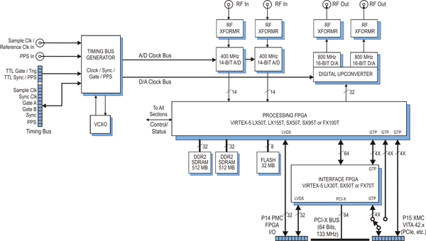
Pentek Model 7156
Https Ieeexplore Ieee Org Iel7 8740845 8742804 08742858 Pdf
